-
ASIC
The ASIC is a high-density array of low-noise amplifier circuits that is used to measure and provide a digital readout of the current flow in the electrochemical circuit between the individual well and shared common electrode. In addition, the ASIC receives commands from the host software system to provide control functionality for the sensor array, including: acquisition frequency, signal filtering, sensor current range, multiplex input selection, electrode bias potential generation, and deselection of sensor inputs with broken membranes to avoid saturation of the measurement circuits.
The flow cell ASIC is designed to operate across a wide range of conditions depending on the application. Typical operating cases are acquisition frequency of 2 to 20 kHz while measuring 10s to 1000s of pico-amperes. The applied electrode bias potential can be controlled using scripts in MinKNOW with a range of ± 1 V.
The ASIC also has the ability to use the applied potential to unblock any of the channels that are not sequencing. A reversal of the potential can “flick” any stray DNA or contaminants out of the pore on a per channel basis and reset the channel to an “open pore” state to allow the next strand to be sequenced. This ability is further utilised in “Read Until...” schemes, where the MinION Mk1B and Mk1C can be programmed to responds to a sequence or signature, choosing to either keep or reject the DNA stand in the nanopore on an individual basis, maximising the time to results and allowing the user to change the priority of sequencing during a run.

-
Channel layout
The MinION Mk1B and Mk1C/GridION flow cell currently has 2048 active well electrodes organised hexagonally on the surface of the array. The active wells are arranged in two blocks of 32x32 with a set of four inactive wells separating them. There are also inactive wells present at the edges of the array where the gasket sits.
The channel map is shown below, viewing the sensor chip from the top with the fluid inlet (or common connection pin) to the left of the sensor.

Layout:
- The current hexagonal packing is a result of the horizontal offset of alternative rows and the original chip design evolving from a square array
- There is a section of four columns in the middle where there are wells on the surface of the chip, but these wells are not connected to the ASIC (black hexagons)
- There are also some redundant wells around the edges of the sensor (black hexagons)
Basic numbers:
- 2048 sensor wells available (64 x 32)
- 512 measurement channels, 4x Multiplexing (MUX), see the MUX scan below.
Features:
- Channels 1-64 occur at the top of the chip (the other low channel numbers are at the bottom)
- Channels order down the chip: 1-64, 449-512, 385-448, 321-384, 257-320, 193-256, 129-192, 65-128
- MUXs run from left to right in the order: 3, 4, 1, 2, 2, 1, 4, 3
-
Relationship between nanopore sensors and ASIC channels
The ASIC is capable of recording through all channels simultaneously, with the 2048 active well electrodes organised in groups of four. The choice of a single well for each of the recording channels is referred to as multiplexing. Multiplexing the nanopore array is used to improve the yield of channels containing a single pore and the sequencing output of the consumable. Is it common to see data provided with ‘channel’ and ‘MUX’ information. Most sequencing scripts perform a ‘MUX selection’ where the best 512 wells are chosen as the first group. Later groups of wells can be switched to during a sequencing run to provide more output.

-
Sensor array
The sensor area of the flow cell is comprised of many individual sensor wells, each designed to hold a single nanopore. These sensor wells have a micro patterned structure, created using photolithographic techniques, sitting on a silicon substrate. The well provides the geometry for forming a membrane so that a single nanopore can be inserted. The well is approximately 90 μm deep with a platinum electrode at the base of the well. This electrode is then connected to the PCB through vias in the silicon layer. On the top of the wells are pillars of photoresist that are patterned to control the movement of a hydrophobic pretreatment. The wells are also patterned with additional features to control the pretreatment distribution.
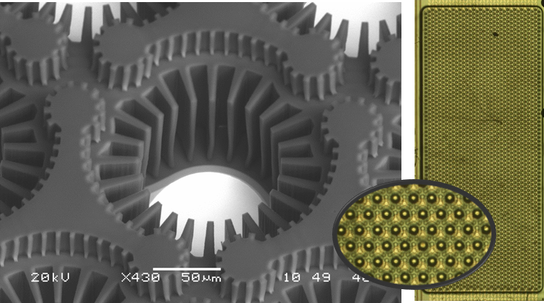
SEM image of a single sensor well (left) and the hexagonal array of wells (right). -
Membranes
For each of the wells, a membrane is formed over the array so that the ionic fluid underneath the membrane is trapped. The membrane provides an insulating layer, so that once a nanopore is inserted, communication between the electrodes is dominated by the signal through that pore. Oxford Nanopore uses a proprietary amphiphilic polymer and a synthetic pretreatment oil to form the membrane. The use of this polymer gives the flow cell membranes increased robustness to physical disruption, chemicals, and biological materials.
-
Electrodes
Electrodes are used to create a circuit with the membrane and the buffer, present in the sensor array, so that electrophysiological measurements can be made as the ion flow changes through the pores.

